In Part 1 we talked about the processes leading up to assembly such as screen printing and optical inspection. The next stage of manufacturing is where precision machinery and our skilled technicians come together to place thousands of tiny components, solder them, and verify every connection. Mistakes here can compromise reliability, so every step is carefully controlled and documented.
Surface Mount Technology (SMT) Assembly
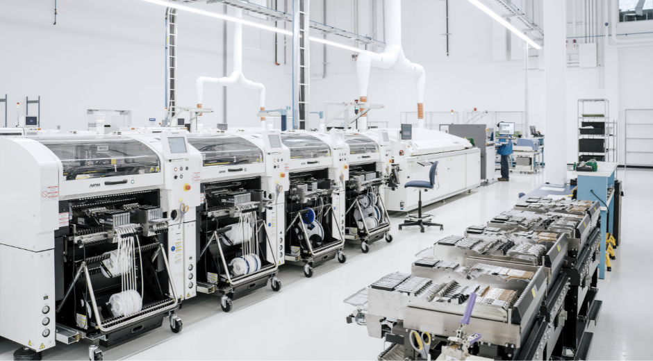
Once solder paste has been applied and passes inspection, the board moves to the SMT line, where each component is precisely aligned with its corresponding solder deposit to ensure proper electrical and mechanical connection. This stage is central to PCB assembly because component placement directly affects solder quality, electrical performance, and long-term reliability. Any misalignment at this stage can lead to defects down the line.

The assembly process relies on Panasonic’s high-speed, multi-functional pick-and-place modules equipped with dual placement heads, each supporting up to sixteen nozzles. These machines can handle components as small as 01005 (Imperial) and 0402 (Metric), smaller than a grain of rice, while also accommodating lead pitches as fine as 0.3 millimeters. They can manage complex packages such as micro-BGA, BGA, CSP, LGA, QFN, QFP, and PoP (Package-on-Package), as well as odd-form components like connectors up to 150 millimeters in length.

Reflow Soldering and Post-Reflow Inspection
After placement, the boards enter BTU International reflow ovens, where the solder paste melts and forms metallurgical bonds between component leads and the board’s copper surfaces. Reflow is a highly technical process that requires precise thermal profiling: the boards must be heated and cooled along exact temperature curves to prevent warping, thermal stress, or solder defects. Different component types, board materials, and densities require customized profiles to balance thermal energy and solder reliability.
Following reflow, boards undergo another inspection before the testing process. Experienced technicians visually examine each board under magnification to identify subtle defects, while X-ray inspection verifies hidden solder joints beneath BGAs or other dense packages where visual inspection is impossible. This combination of inspection methods ensures first-pass yield remains high, reducing the need for costly rework and supporting consistent production quality across complex assemblies.

Through-Hole Assembly
While SMT handles most components, certain parts such as connectors, transformers, and high-current devices must still be manually inserted through the PCB. Our technicians ensure these components are correctly oriented, fully seated, and ready for soldering.

Through-hole boards are completed using either wave soldering or selective soldering depending on the complexity of the assembly. In wave soldering, the entire board passes over a wave of molten solder, simultaneously forming connections on all through-hole joints, which is efficient for high-volume boards with simpler layouts. Selective soldering applies solder only to specific joints using a programmable nozzle, making it suitable for dense layouts, mixed SMT and through-hole boards, or heat-sensitive components. Careful control of solder temperature, dwell time, and flux application is critical in both processes to avoid defects such as cold joints, solder bridging, or incomplete wetting.


Testing and Quality Verification
Once the assemblies are completed, each board undergoes testing to ensure it meets your unique specifications. Our Product Engineers and qualified test technicians collaborate with you to define test protocols that align with your product requirements, ensuring functional and performance standards are achieved before shipment. When custom testing is required, we either use customer-provided units or develop dedicated test platforms based on your instructions. This includes the creation of automated functional test jigs and fixtures tailored to your specifications, enabling repeatable, high accuracy testing across production runs.

Our testing capabilities cover a wide range of technologies, including RF systems, GPS-enabled devices, wireless and wired computing equipment, IR cameras and sensors, and diverse data acquisition devices.
If you would like to learn more or visit our facilities in person, please reach out to sales@dorigo.com to set up a meeting.